
Huawei Y Series Schematic Diagram
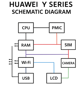
Huawei Y Series Schematic Diagram is a detailed schematic and PCB layout for Huawei Y series smartphones. The guide is designed for repair and service technicians, allowing them to study electrical circuits, component locations, and board layouts. The diagrams help you quickly find faults, check power, repair damaged lines, and perform high-quality component-level repairs.
Huawei Y3 (2017, 2018), Y3 II
Huawei Y5 (various releases: 2017, 2018, 2019), including Y5 II, Y5c
Huawei Y6 (2017), Y6 II, Y6p (2020)
Mid and high segment:
Huawei Y6 (2018, 2019), extended variants with prefixes - Y6s, Y6 Pro (2017), Y6 Prime (2018)
Huawei Y7 (2017, 2018, 2019), Y7p, Y7 Prime (2018, 2019), Y7 Pro (2019)
Huawei Y8p, Y8s
Higher models:
Huawei Y9 (2018, 2019), Y9a, Y9s
Nova Y series models (belongs to Y-series): Nova Y70, Y70 Plus, Y71, Y90, Y91
Also Nova Y8p, Y61, Y72, Y72S, Y73 - all are part of the extended Huawei Y-series lineup
Nova Y70, Y70 Plus, Y71, Y90, Y91, Y8p, Y61, Y72, Y72S, Y73
| Huawei Y520-U22 service schematics | Download |
| Huawei Y600-U00 service schematics | Download |
| Huawei Y9 Prime 2019 Schematic Diagram | Download |
| Huawei Y9 2018 (HL1FLAM) Schematic Diagram | Download |
| Huawei Y7 Prime 2019 Schematics Diagram | Download |
| Huawei Y7 Prime 2018 Schematics Diagram | Download |
| Huawei Y7 2019.Y7 Prime 2019 PCB Layout HL3DUBM | Download |
| Download |
y 8p (Saturday, 27 September 2025 08:19)
schematic diagram
Godday (Saturday, 06 September 2025 21:29)
so sorry sir, it is hauwei y9a am talking about please i need the schematic diagram
Godday (Saturday, 06 September 2025 21:18)
good evening sir please i need gionee y9a schematic diagram