
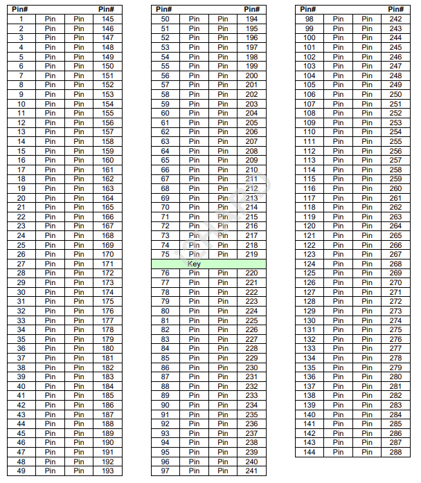
DDR5, GDDR5X Pinout Table
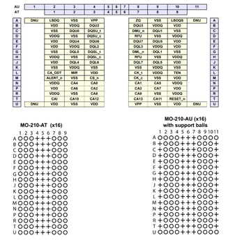
190 ball BGA Package DDR5
GDDR5X

DDR5 pinout
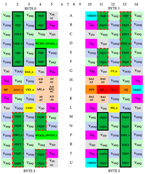
DDR5 SDRAM X16 Ballout Using MO-210
The additional columns and rows of inactive balls in the MO-210 AU (x16) terminal block with support balls are intended for mechanical support only and should not be connected to either high or low electrical levels.
Some additional support balls may be optionally installed at the supplier's discretion. See the supplier's datasheet.
Pinout Description
| Symbol | Type | Function |
|---|---|---|
| CK_i, CK_o | Input | Clocks CK_i and CK_o are differential clock inputs. All address and control input signals are sampled on the crossing of the positive edge of CK_i and negative edge of CK_o. |
| CS_n | Input | Chip Select. All commands are masked when CS_n is sampled HIGH. CS_n provides for external Rank selection on systems with multiple Ranks. CS_n is a combined part of the command code. CS_n is also used to define specific modes in the part by RFU commands. |
| DM_n, DMU_n, DML_n | Input | Input Data Mask. DM_n is an input mask signal for write data. Input data is masked when DM_n is sampled HIGH during a Write access. DMU_n is sampled on both edges of DQS. For all devices, the use of DM_n is mandated by MRS OP[A3]. DM_n are region bits for all devices. |
| CA [9:0] | Input | Command/Address Inputs. CA signals provide the command and address inputs according to the Command Truth Table. Note: Since some commands use Multi-Cycle, the pins may not be interchanged between devices on the same bus. |
| RESET_n | Input | Active Low Asynchronous Reset. Reset is active when RESET_n is LOW, and inactive when RESET_n is HIGH. RESET_n must be HIGH during normal operation. RESET_n via CMDS will not signal with DC High and low as BPWR and ZOPR, or VDDQ. |
| DQ | Input / Output | Data Input/Output. Bi-directional data bus. If CRC is enabled via Mode register then CRC code is added at last 8-bits of burst. |
| DQS_t, DQS_c, DQSU_t, DQSU_c, DQSL_t, DQSL_c | Input / Output | Data Strobe. output with read data, input with write data. Edge-aligned with read data, centered in write data. For the x16, DQS2L corresponds to the data on DQS1-DQ2_t. DQS2 corresponds to the data on DQS1O-DQS17. The data strobes DQS_t, DQS1_t, and DQS1_t correspond with differential signals DQS_c, DQS1_c, and DQS1_c, respectively, to provide differential pair signaling to the system during reads and writes. DQRS EDM provides a differential data strobe, only and does not support a single-ended. |
| TDQS_t, TDQS_c | Output | Termination Data Strobe. TDQS_t/TDQS_c is applicable for x8 DRAMs only. When enabled via MRS OP[A3], the DRAMs shall provide the same termination/resistance function as TDQS_t/TDQS_c, that is applied to DQS_t/DQS_c. When disabled via MRS OP[A3], DM_n/TDQS_t shall provide the Dual Mask function depending on MRS OP[5]. TDQS_c is not used. x4,x16 DRAMs must disable the TDQS function via MRS OP[4]. |
| ALERT_n | Input / Output | Alert! If a CRC error is detected, ALERT_n goes LOW for a time interval and goes back HIGH. During Connectivity Test mode, this pin wakes up an input. Optional use of this signal is dependent on the system. If the ALERT_n is not used, the ALERT_n pins must be pulled to VDDQ on the board. |
| TEN | Input | Connectivity Test Mode Enable. Required on x16, x8 & x32 devices. HIGH in this pin shall enable Connectivity Test Mode operation along with other pins. It is a CMOS rail-to-rail signal with AC High and low at BPWR and ZOPR, or VDDQ. Using this signal or not is dependent on System. This pin may be DCM active in regular operation through a weak pull-down resistor to VSS. |
| MR | Input | Mirror. Used to select SGRAM mode that if the Mss is being configured for Mirrored mode. In Standard mode. With the MR pin connected (strapped) to VDDQ, the SGRAM internally swaps even numbered CA with the next higher odd number CA. Normally the MR pin must be tied to VSS or CA mode in Standard. Mirror use generates CA2 with CA3 (not CA1) CA4 with CA5 (not CA3). Note that the CA0/1 function is only relevant for certain devices (including electrical). If DRAMs are present, it is the case that CA10 is not used. In tall solution, considering whether MR is used or not, should be compared (strapped) to VDDQ. No active signaling requirement defined. |
| CAI | Input | Command & Address Inversion. With the CAI pin connected (strapped) to VDDQ, DRAM internally inverts the logic-level present on all the CA signals. Normally the CAI pin must be connected to VSS if no CA inversion is expected. No active signaling requirement defined. |
| CA_DCP | Input | LSDT for Command and Address. Apply Group B settings if the pin is connected (strapped) to VSS and apply Group B settings if the pin is connected (strapped) to VDDQ. No active signaling requirements defined. |
| LBDS | Output | Loopback Data Output. The output of this device on the Loopback Output Select declared in MRS3 OP[A2]. When Loopback is enabled, it is in driver mode using the default BOM described in the Loopback Function section. When Loopback is disabled, the pin is either terminated at RZ based on MRS3/OP[2:0]. |
| LBDQS | Output | Loopback Data Strobe. This is a signal ended strobe with the falling edge aligned with Loopback data edges. Left-aligned with read data, right-aligned with loopback select strobe. It is in driver mode using the default BOM described in the Loopback Function section. When Loopback is disabled, the pin is either terminated at RZ based on MRS3/OP[2:0]. |
| RFU | Input / Output | Reserved for future use. |
| NC | - | No Connect. No internal electrical connection is present. |
| VDDQ | Supply | I/O Power Supply 1.1V |
| VDD | Supply | Power Supply 1.1V |
| VSS | Supply | Ground |
| VPP | Supply | DRAM Activating Power Supply 1.8V |
| ZQ | Reference | Reference Pin for ZQ calibration. This ball is tied to an external ZQ (240 ohm resistor)(RZQ), which is tied to VSS. |
Comments: 0